Table of Contents >> Show >> Hide
- Introduction: The Tiny Ingredient That Changes Everything
- What Is a Semiconductor Dopant?
- Why Hobbyists Care About Doping
- The Core Design Questions
- Industrial Doping Methods: Useful to Know, Not Always Wise to Copy
- A Safer Hobbyist Design Framework
- Key Design Parameters for a Hobbyist Dopant Concept
- What a Hobbyist Can Realistically Build
- Common Mistakes in Hobbyist Semiconductor Doping Projects
- Specific Example: A Safe Educational Dopant Study
- Designing for Documentation
- Experience Notes: What Designing A Hobbyist’s Semiconductor Dopant Teaches You
- Conclusion: The Best Hobbyist Dopant Is a Thoughtful Design
- SEO Tags
Note: This article is written for educational publishing. Semiconductor doping involves heat, toxic chemicals, specialized equipment, and strict safety controls, so the discussion below focuses on design thinking, concepts, and safe hobbyist learning paths rather than a do-it-yourself lab procedure.
Introduction: The Tiny Ingredient That Changes Everything
In the world of electronics, a semiconductor dopant is the microscopic equivalent of adding one drop of hot sauce to a giant pot of soup. Use too little and nothing interesting happens. Use too much and the whole recipe changes personality. Dopants are carefully chosen impurity atoms added to materials such as silicon to change how easily electrons move through them. That sounds simple, but it is one of the main reasons modern electronics exist.
Without doping, silicon is useful but not magical. With doping, silicon becomes the foundation for diodes, transistors, solar cells, sensors, integrated circuits, and the small black rectangles that quietly run half of civilization. Designing a hobbyist’s semiconductor dopant project, then, is not about casually sprinkling chemicals on a wafer and hoping for the best. It is about understanding the physics, the safety limits, the measurement challenges, and the realistic ways a curious maker can explore the subject without turning the garage into a low-budget villain laboratory.
This guide explains how a hobbyist can think about semiconductor doping: what dopants do, what design goals matter, which approaches are realistic, which ones belong in professional facilities, and how to learn from the process without pretending that a kitchen table is a cleanroom.
What Is a Semiconductor Dopant?
A semiconductor is a material whose electrical conductivity sits between a conductor and an insulator. Silicon is the celebrity of this category because it is abundant, stable, and compatible with highly refined manufacturing processes. Pure silicon forms a crystal lattice where each atom shares electrons with neighboring atoms. That structure is elegant, but by itself it does not provide enough free charge carriers for most electronic devices.
A dopant changes that. By introducing a small number of atoms from nearby groups on the periodic table, engineers can create extra electrons or electron “holes.” These charge carriers make the material more conductive and allow device designers to control current flow with astonishing precision.
N-Type and P-Type Doping
In silicon, common n-type dopants include phosphorus, arsenic, and antimony. These atoms have one more valence electron than silicon, so they can donate an electron to the crystal. The result is n-type material, where electrons are the majority carriers.
Common p-type dopants include boron, aluminum, gallium, and indium. These atoms have one fewer valence electron than silicon, creating holes that behave like positive charge carriers. The result is p-type material, where holes are the majority carriers.
Put p-type and n-type regions next to each other and you get a p-n junction, the essential building block of diodes, bipolar transistors, many sensors, and solar cells. That junction is the “one-way door” that makes modern electronics possible. Not bad for impurity atoms that would be rude guests in almost any other crystal.
Why Hobbyists Care About Doping
For most hobbyists, semiconductor doping is less about producing commercial chips and more about understanding the hidden craft behind electronics. Anyone can buy a microcontroller for a few dollars. Understanding why its transistors work is a different level of curiosity.
A hobbyist’s semiconductor dopant project may aim to demonstrate a diode, modify the resistance of a silicon sample, explore p-type and n-type behavior, compare wafer resistivity, or build intuition about fabrication. The goal is rarely to compete with a fabrication plant. A modern fab has billion-dollar facilities, ultra-clean environments, ion implantation tools, process controls, metrology systems, and teams of people who know what every alarm means. A hobbyist has enthusiasm, patience, thrift, and possibly a multimeter that has been dropped twice.
That difference matters. The best hobbyist design is realistic. It respects safety, avoids unnecessary hazards, and focuses on measurable learning rather than heroic overreach.
The Core Design Questions
Designing a hobbyist’s semiconductor dopant starts with questions, not chemicals. A good project plan should answer what material is being studied, what electrical change is expected, how the change will be measured, and what risks must be avoided.
1. What Material Are You Working With?
Silicon is the obvious choice because it is widely used and educationally rich. However, hobbyists can also learn from germanium diodes, pre-doped wafers, solar cells, or semiconductor experiment kits. Starting with pre-doped material is often the smartest path because it allows testing and comparison without introducing hazardous dopant sources.
2. What Type of Doping Do You Want to Understand?
The key distinction is n-type versus p-type. A project may compare the behavior of n-type and p-type wafers, examine rectification in a diode, or measure changes in resistance across samples. The design goal should be stated in electrical terms, not just chemical terms. “I want to understand how dopant concentration affects sheet resistance” is more useful than “I want to put phosphorus into silicon.”
3. How Will You Measure Success?
Measurement is where semiconductor dreams either grow up or trip over their shoelaces. A visual change is not enough. Doped silicon often looks like regular silicon, which is rude but normal. Hobbyists need electrical measurements such as resistance, sheet resistance, diode current-voltage behavior, or Hall effect data when available.
4. What Safety Boundary Will You Not Cross?
This is the most important design question. Industrial doping can involve toxic gases, corrosive chemicals, high temperatures, radiation hazards, vacuum systems, and waste disposal issues. A hobbyist project should avoid hazardous dopant gases such as phosphine, arsine, and diborane, as well as dangerous wet chemistry such as hydrofluoric acid. Curiosity is excellent; preventable exposure is not a personality trait.
Industrial Doping Methods: Useful to Know, Not Always Wise to Copy
Professional semiconductor manufacturing mainly uses diffusion and ion implantation to introduce dopants. Understanding these methods helps hobbyists appreciate what they are trying to model or observe.
Thermal Diffusion
Diffusion uses heat to drive dopant atoms into silicon. In professional settings, wafers are placed in controlled furnaces where dopant sources, temperature profiles, ambient gases, and time are tightly managed. Dopant atoms move from the surface into the crystal, creating a concentration profile that depends on many variables.
From a hobbyist design perspective, diffusion is conceptually appealing because it sounds straightforward: heat plus dopant source equals doped material. In reality, the details are demanding. Temperature uniformity, contamination control, oxide layers, surface preparation, and measurement all matter. A slightly dirty sample can teach you more about dust than semiconductors, which is not the noblest branch of physics.
Ion Implantation
Ion implantation accelerates dopant ions and shoots them into the wafer. It allows excellent control over dose and depth, which is why it became a cornerstone of advanced chip manufacturing. After implantation, the wafer typically requires annealing to repair crystal damage and electrically activate dopants.
For hobbyists, ion implantation is usually not realistic. The equipment is complex, expensive, and associated with serious safety controls. However, the concept is worth understanding because it explains why modern chips can have extremely precise regions of different conductivity.
Spin-On and Solid Dopant Sources
Some educational and research settings use dopant-containing films or solid sources that are later driven into silicon by heating. These approaches may seem more accessible than gas systems, but they still require chemical safety knowledge, ventilation, temperature control, compatible materials, and responsible waste handling. They should be treated as laboratory materials, not craft supplies.
A Safer Hobbyist Design Framework
The safest and most productive hobbyist approach is to separate learning goals from hazardous processing. Instead of asking, “How do I make a dopant source at home?” ask, “How can I explore doped semiconductors with safe, available materials?” That shift keeps the project educational and practical.
Use Pre-Doped Silicon Wafers
Pre-doped wafers are available from educational suppliers and surplus sources. A hobbyist can purchase n-type and p-type wafers with known resistivity ranges, then compare their electrical behavior. This avoids the hardest and riskiest step while preserving the core lesson: dopant type and concentration affect conductivity.
Build Measurement Skills First
Before attempting any material modification, learn how to measure. A four-point probe setup can reduce contact resistance errors when measuring sheet resistance. A simple current-voltage test can show diode behavior. Hall effect measurements can reveal carrier type and carrier concentration, though they require more specialized equipment.
This measurement-first approach is underrated. In semiconductor work, making a change is only half the challenge. Proving what changed is the other half. Without measurement, a project becomes a science-themed guessing game with better vocabulary.
Explore Diodes and Solar Cells
Commercial diodes and solar cells provide safe windows into doping. A diode contains a p-n junction. A solar cell is essentially a large-area semiconductor device designed to convert light into electrical energy. Measuring their current-voltage curves under different conditions can teach junction behavior, forward bias, reverse bias, leakage, and illumination effects.
Use Simulation Tools
Simulation is not cheating. It is how many real engineers save time, money, and eyebrows. Semiconductor device simulators, circuit simulators, and educational models can show how dopant concentration affects depletion width, threshold voltage, resistance, and junction behavior. A hobbyist can design a virtual dopant profile and compare expected behavior with real components.
Key Design Parameters for a Hobbyist Dopant Concept
If you were designing a safe educational dopant project on paper, several parameters would define the plan.
Dopant Species
The dopant species determines whether the material becomes n-type or p-type. Phosphorus and boron are classic examples for silicon, but the practical handling of actual dopant compounds is a separate matter. In a hobbyist design, the “dopant species” may simply be represented by pre-doped wafers labeled n-type or p-type.
Dopant Concentration
Dopant concentration affects conductivity. Lightly doped silicon behaves differently from heavily doped silicon. Higher dopant levels generally increase carrier concentration, but they can also influence mobility, junction behavior, and leakage. The relationship is not always perfectly linear because crystal defects, compensation, and carrier scattering can complicate the picture.
Depth Profile
A dopant profile describes how concentration changes with depth. Diffusion often produces a concentration that is highest near the surface and decreases inward. Ion implantation creates a more controlled distribution below the surface. Hobbyists may not measure depth profiles directly, but the concept helps explain why sheet resistance and junction behavior depend on more than surface appearance.
Activation
Dopant atoms must occupy electrically useful positions in the crystal lattice to contribute carriers. In industrial processes, activation is closely tied to heat treatment and defect repair. This is one reason professional fabrication is so controlled: simply introducing atoms is not enough. They have to be in the right place, in the right form, with the surrounding crystal still functional.
Contamination Control
Semiconductor fabrication is allergic to randomness. Sodium, metals, particles, moisture, and organic residue can all affect results. A hobbyist may not have a cleanroom, but basic contamination awareness still matters. Handle wafers carefully, store samples properly, label everything, and do not mistake fingerprints for process innovation.
What a Hobbyist Can Realistically Build
A realistic project might involve comparing an n-type wafer, a p-type wafer, a diode, and a solar cell. The hobbyist could measure resistance, observe diode curves, test light response, and document how carrier behavior changes across devices. This kind of project is safe, affordable, and deeply instructive.
Another project could focus on making a simple four-point probe fixture for educational measurements. The design would emphasize consistent probe spacing, gentle contact force, stable current sourcing, and repeatable voltage measurement. Even if the results are not laboratory-grade, the builder learns why contact resistance matters and why semiconductor metrology is a discipline of its own.
A third project could combine simulation and measurement. The hobbyist models a p-n junction in software, predicts a current-voltage curve, then compares it with a real diode. The point is not to beat a professional device simulator. The point is to connect equations, materials, and actual measurements.
Common Mistakes in Hobbyist Semiconductor Doping Projects
Mistake 1: Treating Doping Like Painting
Dopants do not work like paint. A surface coating is not automatically an electrically active doped region. Semiconductor doping depends on atomic placement, crystal structure, thermal history, and activation. If the dopant is not incorporated correctly, the wafer may look impressive and behave like a decorative coaster.
Mistake 2: Ignoring Measurement Error
Two metal clips and a multimeter can produce a number, but not every number is meaningful. Contact resistance, oxide layers, pressure, geometry, and sample thickness can all distort results. Better measurement design often teaches more than more aggressive processing.
Mistake 3: Underestimating Safety
Semiconductor manufacturing has a reputation for precision, but it also involves serious hazards. Toxic dopant gases, corrosive acids, high-energy systems, and high-temperature equipment belong in controlled environments. A hobbyist should design around those hazards, not toward them.
Mistake 4: Expecting Modern Chip Results
Making a working transistor at home is possible only for a tiny number of extremely skilled experimenters with unusual equipment, patience, and safety discipline. Making a modern integrated circuit is a different universe. A good hobbyist project should celebrate learning, not compare itself to a commercial fab that has more sensors than some airports.
Specific Example: A Safe Educational Dopant Study
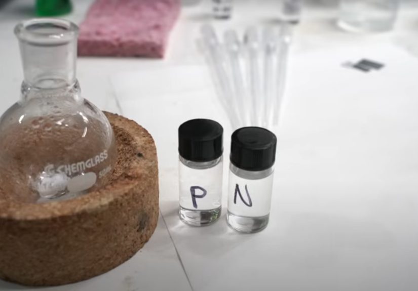
Imagine a hobbyist wants to understand how dopant type affects silicon behavior. A safe design could use three samples: an n-type silicon wafer, a p-type silicon wafer, and a commercial silicon diode. The goal is to compare conductivity and junction behavior without handling dopant chemicals.
The project begins by documenting each sample: type, supplier information, approximate resistivity, thickness, and visible condition. The hobbyist then measures resistance in a consistent geometry and records results. If a four-point probe fixture is available, sheet resistance measurements can be compared across samples. Next, the hobbyist measures the diode’s current-voltage curve by applying small controlled voltages and recording current. The result should show forward conduction and reverse blocking behavior.
To add depth, the hobbyist can simulate a p-n junction and adjust virtual doping levels to see how the depletion region and current flow change. The measured diode data can then be compared with the model. This project does not create a new doped region, but it teaches the essential relationship between dopants and device behavior. It is also much less likely to set off smoke alarms, which is a major advantage in both science and domestic diplomacy.
Designing for Documentation
Good hobbyist semiconductor work needs a lab notebook, even if the lab is a desk and the notebook has coffee stains. Record sample details, measurement conditions, instrument settings, room temperature, probe geometry, and every unexpected observation. Semiconductor behavior can be sensitive to small differences, so documentation turns confusion into data.
Photograph the setup. Save measurement tables. Repeat tests. Compare results on different days. If readings change, investigate why. Was the contact better? Was the oxide layer scratched? Did the sample move? Did the instrument warm up? These questions are not annoying side quests. They are the actual game.
Experience Notes: What Designing A Hobbyist’s Semiconductor Dopant Teaches You
The first experience most hobbyists have with semiconductor doping is surprise. The concept sounds simple: add an impurity and change conductivity. Then you start reading deeper and realize the “impurity” must be selected, placed, activated, measured, and protected from contamination. At that moment, semiconductor manufacturing stops looking like black magic and starts looking like disciplined patience wearing a cleanroom suit.
One of the most valuable lessons is that materials do not care about enthusiasm. A wafer does not become useful because the builder has watched five videos and bought shiny tweezers. It responds to physics. If the surface is oxidized, contacts may behave strangely. If the sample is contaminated, measurements may wander. If the geometry is inconsistent, resistance readings may look like they were generated by a nervous squirrel. This is frustrating at first, but it is also the charm of the topic. It forces careful thinking.
Another experience is learning that safe shortcuts are better than dramatic shortcuts. Using pre-doped wafers may feel less adventurous than attempting a homemade diffusion process, but it often produces better learning. With known n-type and p-type samples, the hobbyist can focus on measurement, comparison, and device behavior. That is where understanding grows. The goal is not to brag about handling dangerous materials. The goal is to understand why controlled impurities create controlled electronics.
Building a simple measurement fixture can be surprisingly satisfying. A four-point probe concept teaches why two-wire resistance measurements can be misleading. Suddenly, contact resistance is not an abstract textbook nuisance; it is the gremlin sitting directly on your data. Once you see that, semiconductor metrology becomes more interesting. You start caring about probe pressure, spacing, repeatability, and sample handling. You become the sort of person who says “sheet resistance” at dinner. This may or may not improve your social life.
The most humbling experience is comparing hobbyist tools with industrial reality. Professional fabs control temperature, particles, gases, humidity, materials, and process history with extraordinary discipline. Their tools can place dopants with precision that is difficult to imagine from a garage bench. Rather than discouraging hobbyists, this should be inspiring. It shows how much knowledge is hidden inside everyday electronics. Every inexpensive diode represents decades of materials science, process engineering, and measurement refinement.
Finally, designing a hobbyist’s semiconductor dopant project teaches respect. Respect for chemistry, because some semiconductor materials are dangerous. Respect for physics, because atoms do not negotiate. Respect for measurement, because a number without context is just decoration. And respect for the people who turned doped silicon into the foundation of modern life. A careful hobbyist may not build the next leading-edge chip at home, but they can build something equally important: real understanding.
Conclusion: The Best Hobbyist Dopant Is a Thoughtful Design
Designing a hobbyist’s semiconductor dopant is less about chasing a risky home-fab fantasy and more about building a smart learning path. Dopants are the tiny ingredients that transform silicon from an interesting material into the heart of electronics. They create n-type and p-type regions, enable p-n junctions, and make diodes, transistors, sensors, and solar cells possible.
For hobbyists, the best design begins with clear goals, safe boundaries, reliable measurement, and realistic materials. Pre-doped wafers, commercial diodes, solar cells, simulation tools, and four-point probe experiments can teach the core ideas without unnecessary hazards. Industrial processes such as diffusion and ion implantation are worth studying, but they should be understood as controlled professional methods, not casual weekend recipes.
The magic of doping is not that impurities exist. The magic is that a few carefully managed atoms can change the behavior of an entire device. That idea is small enough to fit inside a crystal lattice and large enough to power the digital world. For a hobbyist, that is a beautiful place to start.